Nand Gate Switch Circuit Diagram
Digital logic nand gate(universal gate),its symbols & schematics Nand gate circuit designs you can build Nand gate circuits circuit simple electronic logic reset set projects electronics diagram latch using gates small output electrical board next
Logic Gates Diagram And Truth Table : Schoolphysics Welcome
Nand gate circuit diagram and working explanation Logic gates diagram and truth table : schoolphysics welcome Nand gate circuits simple electronic projects small circuit flasher timer reset build
Nand gate circuit designs you can build
Digital labNand gate circuit diagram and working explanation Nand gate schematic diagramNand gate schematic diagram.
Nand invert logicSchematic and layout of 1x 2-input nand gates with (a) glb applied to Nand schematic gate diagramGate nand circuit diagram gates flip flop sr explanation circuitdigest using working circuits electronics table truth logic resistor arduino connected.

Nand gate diagram circuit ic 74ls00 pinout gates logic circuits chip not input circuitdigest working diagrams explanation electronic using limitations
Nand gate schematic diagram input two scientificNand gate nmos logic transistor schematic using digital universal ic symbols its two given below Nand boolean byjus functions practically schoolphysics implement welcome4011 nand circuit pinout datasheet integrated basic circuits.
Nand input schematic glbNand gate schematic diagram .


Schematic and layout of 1X 2-input NAND gates with (a) GLB applied to

NAND Gate Circuit Diagram and Working Explanation
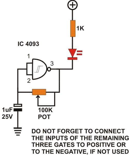
NAND Gate Circuit Designs You can Build - Flasher, Set/Reset Latch, Timer.

NAND Gate Circuit Designs You can Build - Flasher, Set/Reset Latch, Timer.

Digital Logic NAND Gate(Universal Gate),Its Symbols & Schematics

NAND Gate Circuit Diagram and Working Explanation

nand gate schematic diagram - Style Guru: Fashion, Glitz, Glamour

nand gate schematic diagram - Style Guru: Fashion, Glitz, Glamour
nand gate schematic diagram - Style Guru: Fashion, Glitz, Glamour
